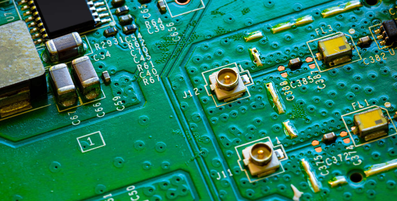
Printed Circuit Boards (PCBs) are the backbone of modern electronic devices, serving as the platform that connects and supports various electronic components. Among the many critical aspects of PCB design, transmission lines play a pivotal role in ensuring the integrity and performance of high-frequency signals. In this blog, we will delve into what PCB transmission lines are, why they are important, and how they influence the overall performance of electronic devices.
What is a PCB Transmission Line?
A PCB transmission line is a specialized conductor layout on a PCB designed to carry high-frequency signals with minimal loss and distortion. Transmission lines ensure that signals travel from one point to another without significant degradation. They are crucial in applications where signal integrity is paramount, such as in RF (radio frequency), microwave, and high-speed digital circuits.
Types of PCB Transmission Lines
There are several types of transmission lines used in PCB design, each suited for different applications and requirements:
Microstrip Line:
- Description: A conductor trace on the top layer of a PCB with a reference ground plane on the bottom layer.
- Applications: Widely used in RF and microwave circuits due to its simplicity and ease of implementation.
Stripline:
- Description: A conductor sandwiched between two ground planes within the PCB.
- Applications: Preferred in high-speed digital and RF applications for its superior signal integrity and reduced electromagnetic interference (EMI).
Coplanar Waveguide (CPW):
- Description: A conductor flanked by two ground planes on the same layer, with or without a bottom ground plane.
- Applications: Used in microwave circuits where reduced signal loss and tight control of impedance are required.
Differential Pair:
- Description: Two parallel traces carrying equal and opposite signals.
- Applications: Commonly used in high-speed digital communications (e.g., USB, HDMI, Ethernet) to reduce noise and crosstalk.
Why Are PCB Transmission Lines Important?
Transmission lines are crucial for several reasons, particularly in high-frequency and high-speed applications:
Signal Integrity:
- Explanation: High-frequency signals are susceptible to loss, distortion, and reflections. Proper transmission line design ensures that signals maintain their integrity, meaning they arrive at their destination without significant degradation. This is essential for maintaining the performance and reliability of the overall system.
Impedance Matching:
- Explanation: Transmission lines are designed to have a specific characteristic impedance, typically 50 ohms or 75 ohms, to match the impedance of the source and load. Impedance matching minimizes reflections and power loss, which is crucial for efficient signal transmission.
Electromagnetic Compatibility (EMC):
- Explanation: Poorly designed transmission lines can lead to excessive electromagnetic interference (EMI), affecting other nearby circuits and devices. Proper transmission line design helps in controlling EMI, ensuring that the PCB complies with EMC standards and regulations.
Minimizing Crosstalk:
- Explanation: In densely packed PCBs, signal traces running close to each other can cause crosstalk, where a signal in one trace induces unwanted signals in another. Transmission lines, particularly differential pairs and coplanar waveguides, are designed to minimize crosstalk, ensuring clean signal transmission.
Frequency Performance:
- Explanation: As frequencies increase, transmission lines become more critical. High-frequency signals can suffer from skin effect, dielectric losses, and dispersion. Transmission lines are engineered to mitigate these effects, enabling reliable performance at higher frequencies.
Designing PCB Transmission Lines
Designing effective PCB transmission lines involves several key considerations:
Trace Width and Spacing:
- Explanation: The width of the trace and the spacing between traces or ground planes significantly impact the characteristic impedance. Precise control of these dimensions is crucial for impedance matching.
Dielectric Material:
- Explanation: The dielectric constant of the PCB material affects the signal propagation speed and impedance. High-frequency designs often use materials with low dielectric loss to reduce signal attenuation.
Layer Stackup:
- Explanation: The arrangement of layers in the PCB (layer stackup) influences the performance of transmission lines. For example, stripline configurations require careful consideration of the distance between the signal layer and the ground planes.
Via Design:
- Explanation: Vias (vertical interconnect accesses) introduce discontinuities in transmission lines, causing reflections and signal loss. Minimizing the use of vias or designing them carefully is essential for maintaining signal integrity.
Termination:
- Explanation: Proper termination (e.g., resistive termination) at the end of transmission lines prevents signal reflections, ensuring clean signal transmission.
Conclusion
PCB transmission lines are fundamental to the performance and reliability of high-frequency and high-speed electronic circuits. Understanding their role and designing them correctly is essential for ensuring signal integrity, minimizing interference, and achieving optimal performance. Whether you are working on RF, microwave, or high-speed digital designs, paying attention to transmission lines can make a significant difference in the success of your project. By carefully considering factors such as impedance matching, trace geometry, and material properties, you can create PCBs that meet the stringent demands of modern electronics.
