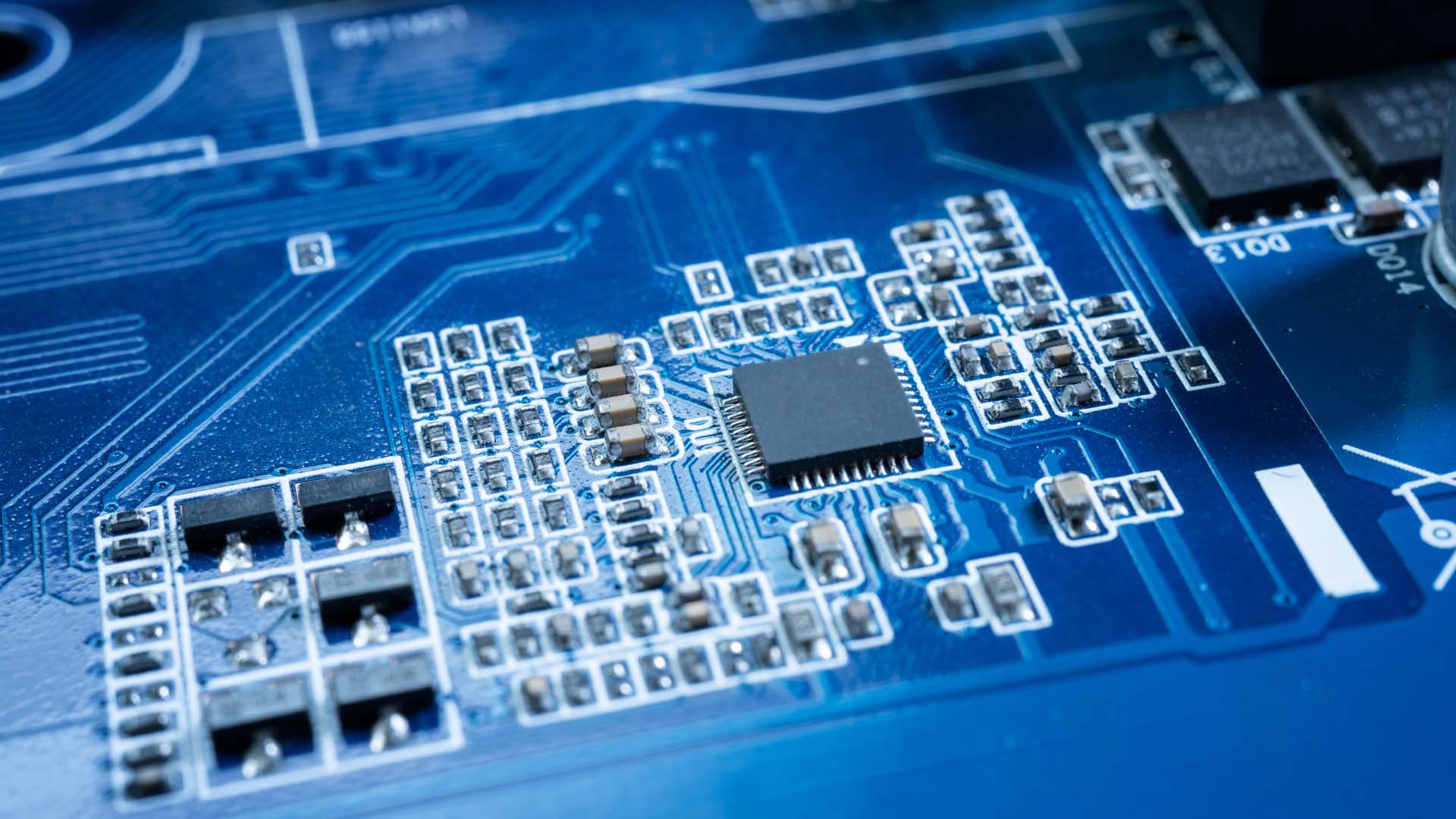
This blog post serves as an in - depth guide for beginners on creating PCB drawings. It details a step - by - step process from schematic creation to Gerber file generation. Additionally, it lists popular PCB design software and answers common questions related to the PCB drawing process, providing a holistic understanding for those new to the field.
Table of Contents
- Introduction
- Step - by - Step Guide to PCB Drawing
- Popular PCB Design Software
- Frequently Asked Questions
- Conclusion
Introduction
In the realm of electronics, PCB (Printed Circuit Board) drawings are the key to bringing electronic concepts to life. They are the bridge between theoretical circuit designs and tangible, functional devices. HHSD Technology, with its commitment to excellence, aims to guide beginners through the intricate process of creating PCB drawings.
Step - by - Step Guide to PCB Drawing
Start with a Schematic
A well - crafted schematic is the foundation of any successful PCB drawing. It is a visual representation of the electrical connections between components, acting as a roadmap for the entire design. Every component and its connection should be carefully planned to ensure the proper functioning of the final PCB.Define the Board Outline
Defining the board outline is crucial as it determines the physical size and shape of the PCB. Considerations such as available space for components and the external enclosure where the board will be placed are essential. A proper board outline sets the stage for efficient component placement.Place Components
The orientation and arrangement of components have a profound impact on the functionality and manufacturability of the board. Group related components together to simplify the routing process and minimize signal interference. This step requires careful planning and foresight.Route Traces
Routing traces is a critical step that involves creating electrical connections between components on the PCB using copper traces. Traces should be as short as possible to reduce signal loss and interference. Avoiding sharp corners in traces is also important to prevent signal reflections.Add Labels and Silkscreen
Labels and silkscreen are used to identify components, test points, and other important information on the PCB. They enhance the readability and maintainability of the board, making it easier for technicians to assemble and troubleshoot.Perform a DRC (Design Rule Check)
A Design Rule Check is an essential step to ensure that the PCB design complies with manufacturing rules. It checks for issues such as minimum trace width, clearance between traces, and proper via usage. Catching and fixing these issues early can save time and resources.Generate Gerber Files
Gerber files are the industry - standard file format used by PCB manufacturers. They contain all the necessary information about the PCB, including copper layers, solder mask, and silkscreen. Once generated, these files can be sent to a manufacturer for production.
Popular PCB Design Software
There are several software options available for PCB design. KiCad is a free and user - friendly option, making it ideal for beginners. Altium Designer, on the other hand, is favored by professionals due to its advanced features and capabilities. HHSD Technology also offers software solutions that are tailored to different user needs.
Frequently Asked Questions
How do I determine the trace width?
The trace width depends on the current flowing through the trace and the acceptable voltage drop. Online calculators can be used to determine the appropriate trace width based on these factors.How can I ensure the manufacturability of my PCB design?
To ensure manufacturability, follow the manufacturer's design rules. Arrange components in an organized manner, use as few vias as possible, and consider making a prototype before mass production. HHSD Technology can provide valuable guidance in this area.How can I avoid signal integrity issues in my PCB design?
To avoid signal integrity issues, keep traces short, avoid sharp corners, and use proper grounding techniques. For high - speed signals, consider using ground planes and controlled impedance traces.How should I route power in a PCB design?
When routing power in a PCB design, use wide traces or power planes to reduce resistance and voltage drop. Separate power and signal traces to minimize interference.
Conclusion
Creating a PCB drawing is a multi - step process that requires attention to detail and a solid understanding of electronics principles. By following the step - by - step guide, choosing the right software, and addressing common questions, beginners can successfully create high - quality PCB drawings.
Are you ready to embark on your PCB drawing journey? Explore the solutions offered by HHSD Technology and take your first step towards creating innovative electronic designs.

